Overall in these 2 weeks we understood what is the difference between anlague and digital sensor and how every sensor could have different creative applications added to the main one that has been fabricated to. That's the fablabs approach, how we could use simple sensors to solve complex problems in a creative way.
For example use a light sensor to know how many times a person has enter a room depending on the change that the light suffers when a person pass by.
Weekly task
You remember when you had to DESIGN A PCB for week 6?
“design a pcb for an input or an output” now it is time to fabricate it ( finish the design - mill it - solder it)
Make the PCB you designed real and make it work ( you have from these week until INPUT WEEK- included)
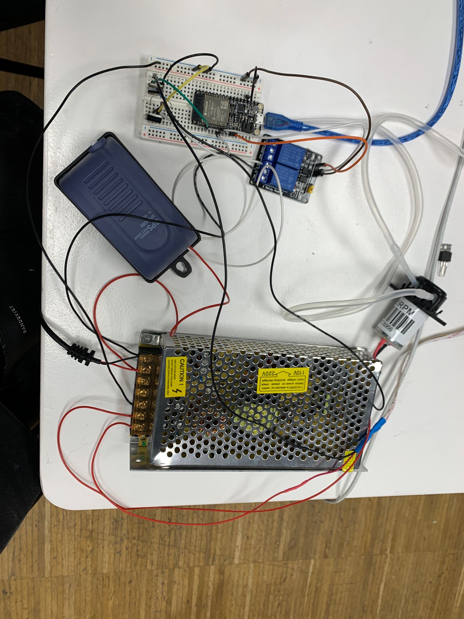
Even though I had already milled the shield for my ESP32 with a thermistor sensor, The prioritise during the upcoming weeks changed a bit. I first started to design a PCB for the 2nd challenge but since I lost it on my laptop I decided to don’t go back to that one. As you can see in the picture we have a lot of wires and connections for the PBR so the smartest thing is to mill a PCB that will make our lives way easier.
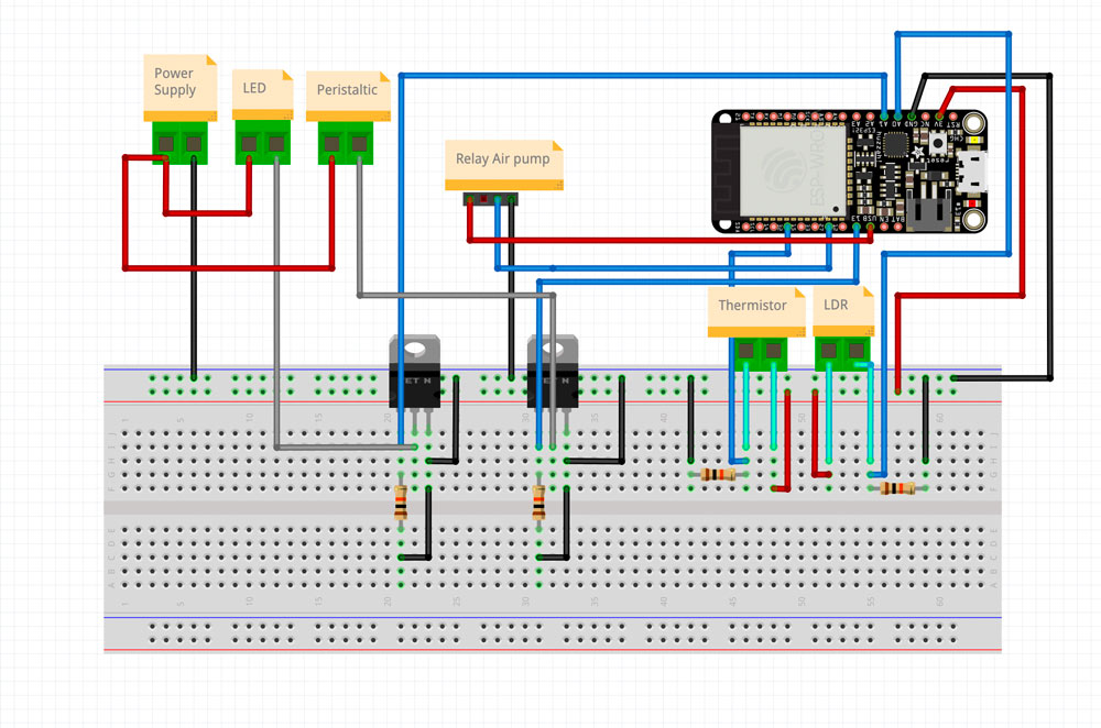
In this case, I decided to use fritzing and try out another software to design the electronic system. Honestly, I found the software a bit annoying. It’s true that it has an interface way more visually appealing than Kicad and to visualize the diagram system with all the connections is really nice. But when it comes to understanding the schematics and designing the PCB with the proper footprints, was a bit tricky and I couldn’t find all the settings to change the clearance.
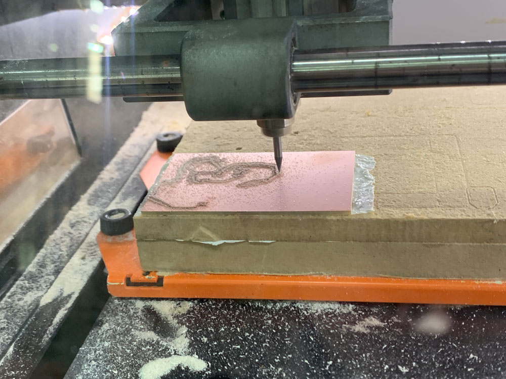
After checking all the connections with Josep, I finally designed the PCB to be milled but since it is a bit of a complex one I asked Edu to double-check that routing was good before going into the milling process. As I said this software was a bit annoying for me, true it exports directly all the different files of the holes and traces but I prefer to check them all on illustrator by layers and make sure that all the parts are well placed. So I have to redo most of the holes which took me a lot of time. Also when I finally had 3 separate files I converted them into Gcode in the Mods project and repeated the process detailed in the week 6 documentation.
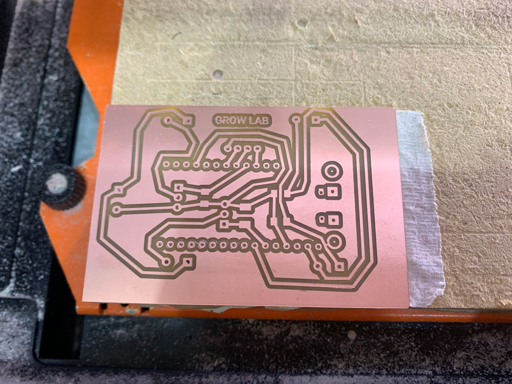
When we send the first board I realized that something was odd. Even though it was the 5th PCB that I milled, I learned that you can never take anything for granted. The outline contrast of the file didn’t have enough space which was not possible to read for mods project and it didn’t create the gcode for a tiny bit of the line, if it was only the outline it would have been fine but the problem was that the traces on the sides of the PCB weren’t properly closed and even though I checked one by one every trace around the holes, I assumed that the sides were alright. Anyway, we adjusted the drawing and repeated the process again. And look what a beautiful plate we made, yes, yes… you can call me PCB Queen.

Soldering all the components and testing the final pcb out. We had another ‘problem’ as I said fritzing is not my best friend. The footprint of the wholes for the terminal block didn’t have the separation as the same components that we had so Josep and I decided to bend a bit the legs and just fit them like this. I have to recognize that when soldering the mosfet I struggled a bit and sadly I broke one of the traces that had to repair by adding a jumping wire. I’m a bit sad with the final look of this PCB, if I have more time I will repeat it again and have it all properly placed, but at the same time I didn’t want to waste more material so I decided to go for it for now.


After checking all the connections with the multimeter I finally got all the wires connected to the PCB and tadaaa It works! I can’t believe it!