This weekly class was a full review of all the main components we have to know when designing a PCB. How to read schematics, Datasheets and build our own. It was a bit hard to follow because many all the names were new to me but I decided to be extra focused and take notes of everything to try to understand it as best as I could. For now, I do feel that electronics are gonna be a bit easier for me than 3D modelling, but I won't quit so easily in either of them.

Weekly task
Design a PCB board also called breakout-board for your ESP32 HUZZAH 32 micro controllers ( or other board that you want to use Rapberri pi ,etc) that allows you to connect an input (sensor) or an output (actuator) to your commercial board without cables.Include the design files in your webpage and explain well the process on how you did it.
I have decided to again use the weekly task in order to achieve my purposes of becoming a Bioborg. In this case I wanted to design PCB for a body temperature sensor MAX30205. I founded online some resources were other people explained their projects using this sensor:
Reference 1
Reference 2. I also needed to find the data sheet of the component and of course the symbols and footprint libraries which I found on a website called SnapEDA. After realising that it would take more than3 weeks for the sensor to arrive, I asked Edu if I had chosen the right sensor for my purposes. To what he replied that I could use the thermistor sensor included in our smart citizen kit for this first prototype. I was at first both frustrated and relieved since I had already spent quite some time understanding the MAX30205 sensor.
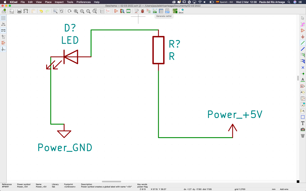
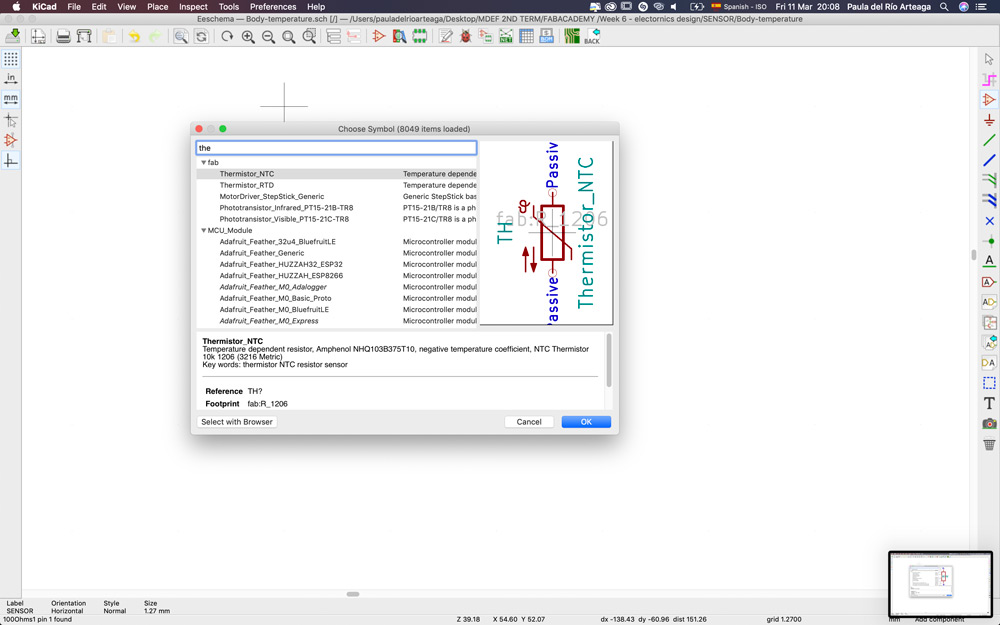
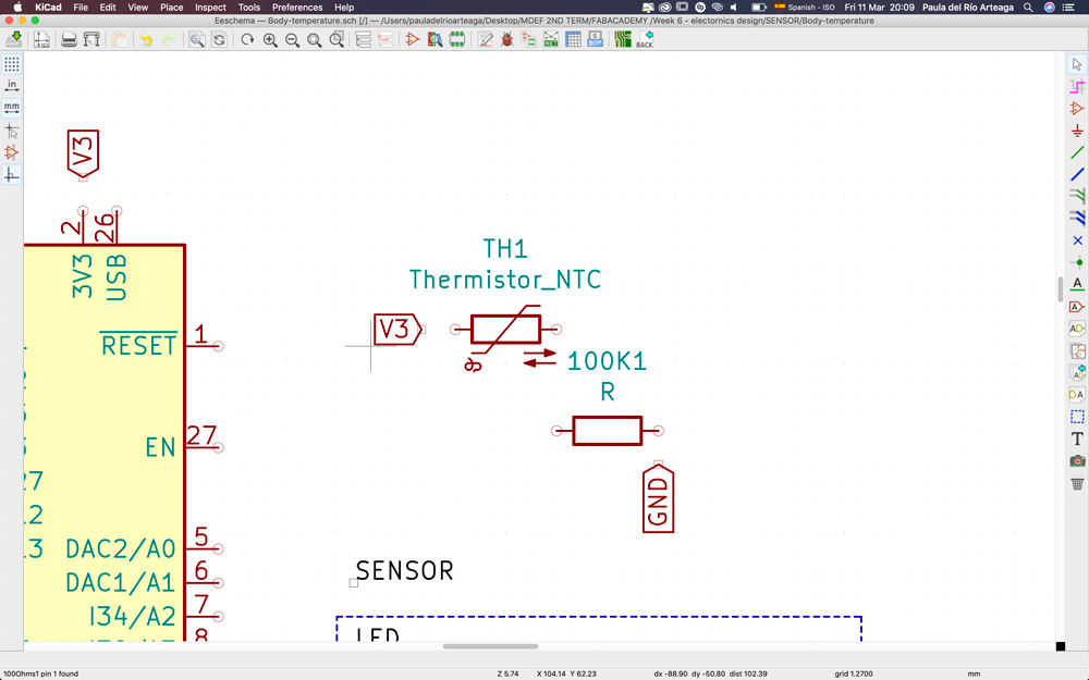
In order to design the circuit to the thermistor sensor I followed a diagram I found online and I decided to also add a Led to the circuit to make it a bit more interactive.
Step by step Body temperature electronics design
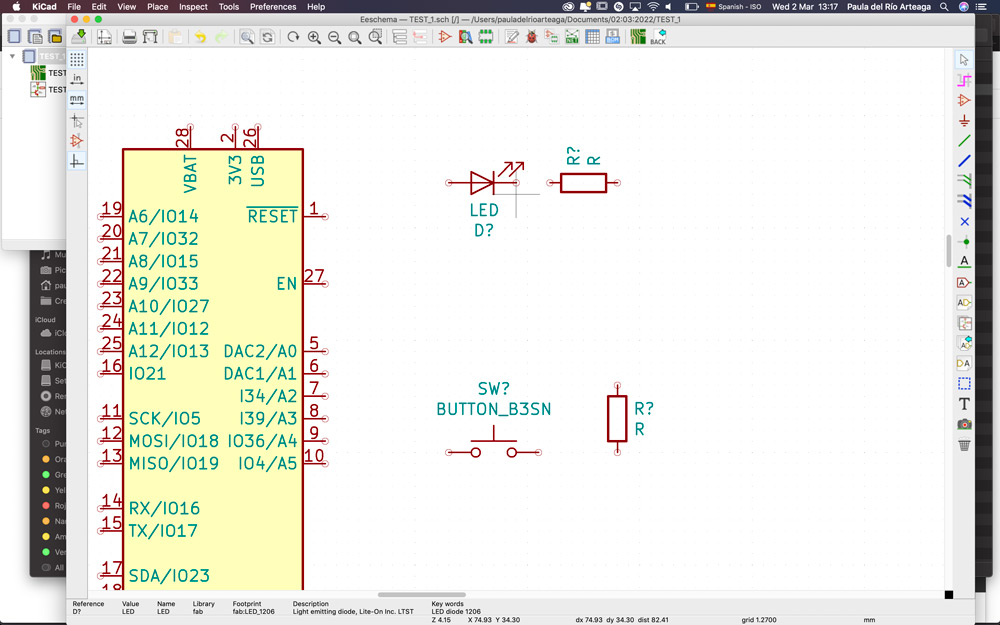
1. Thanks to the datasheet I understood where the pins for connecting my ESP32 to the Thermistor sensor shield has to be.
2. Create a new project on Kicad
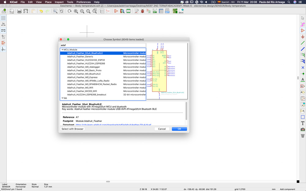
3. Updated the symbols library to Kicad.
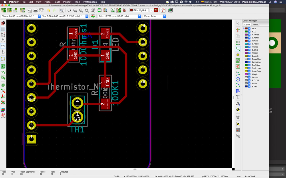
4. Placing the components on the schematics board.

5. Create labels to be able to connect the elements more neatly.
6. Connecting the cables.
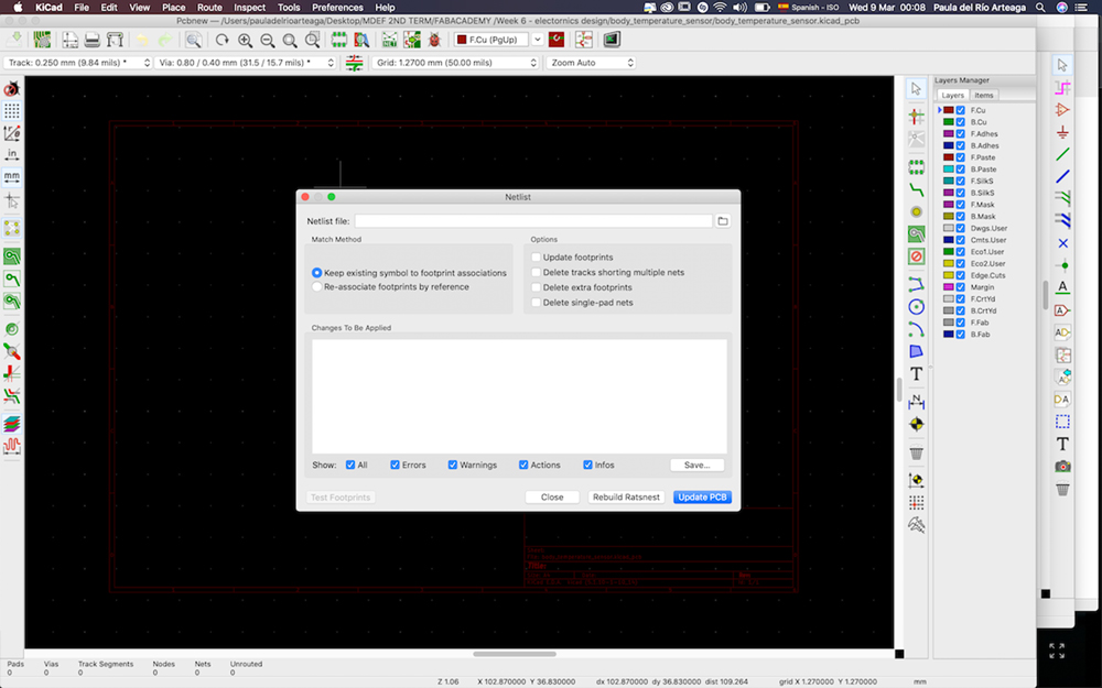
7. Generating nets.


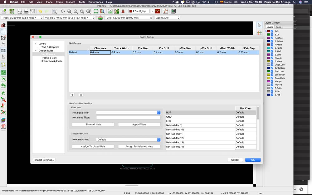
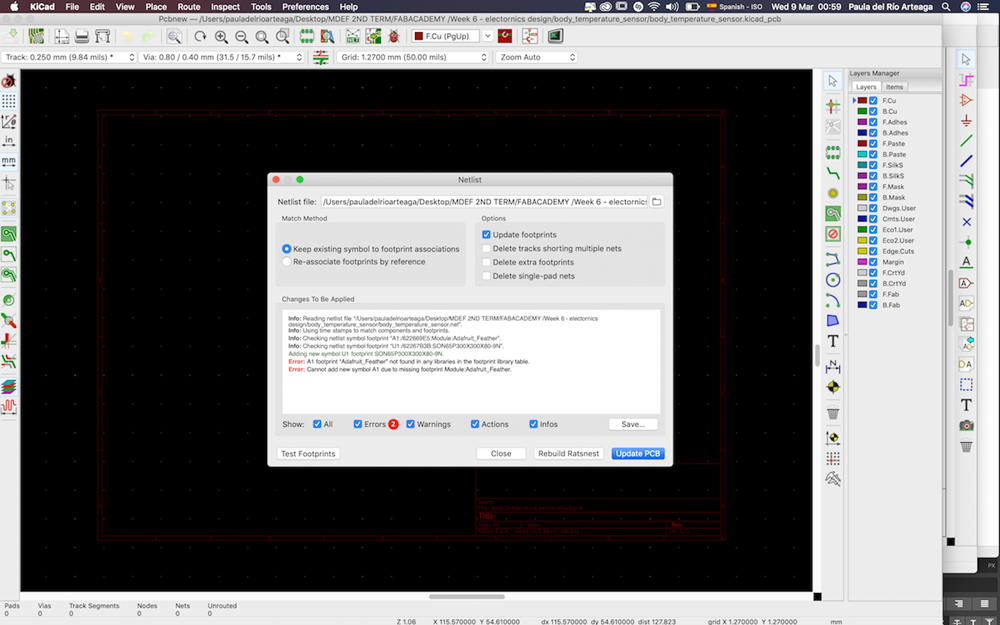
8. Open the physical PCB design and update the generated net.
9. I have an error of the symbols library that does not find Adafruit ESP32 which is weird because I used it in class.
10. Going to the Kicad site to download the module library again and check the route of the libraries again. The problem persisted so I deleted the libraries from Kicad and upload them again with a new name.
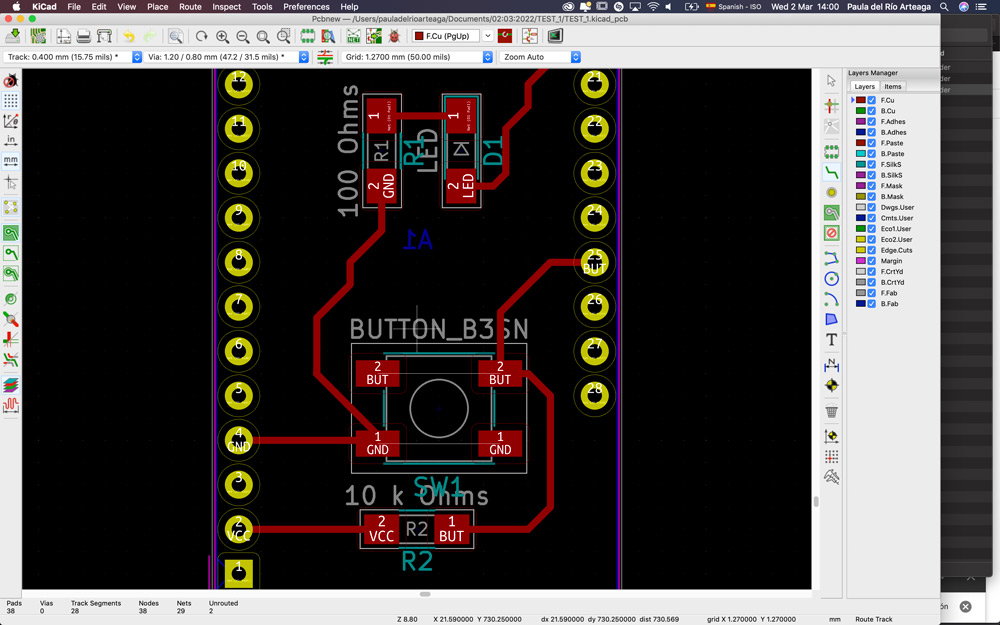
11. Place the components in order. Using the key R we can rotate the component till finding the most optimized position.
12. Since the shield goes on to our microcontroller, we need to invert the drawing.
13. Draw the cables links in the most optimized way possible. Don’t create sharp corners, when drawing the paths. Meaning not having 90º degrees corners.
14. Once every component is properly connected export the file in SVG.

15. Afterwards I opened the file in Illustrator and saved it in 3 different files, outlines, holes and traces in PGN. You can add any designs to it, but for now I wanted to keep it simple.
16. Remember! For the traces invert the colours.
17. Open Modsproject.org and save each file with the corresponding parameters. Important settings coordinates at 0,0,0. Jog height 10 mm. Home 0,0,40mm.


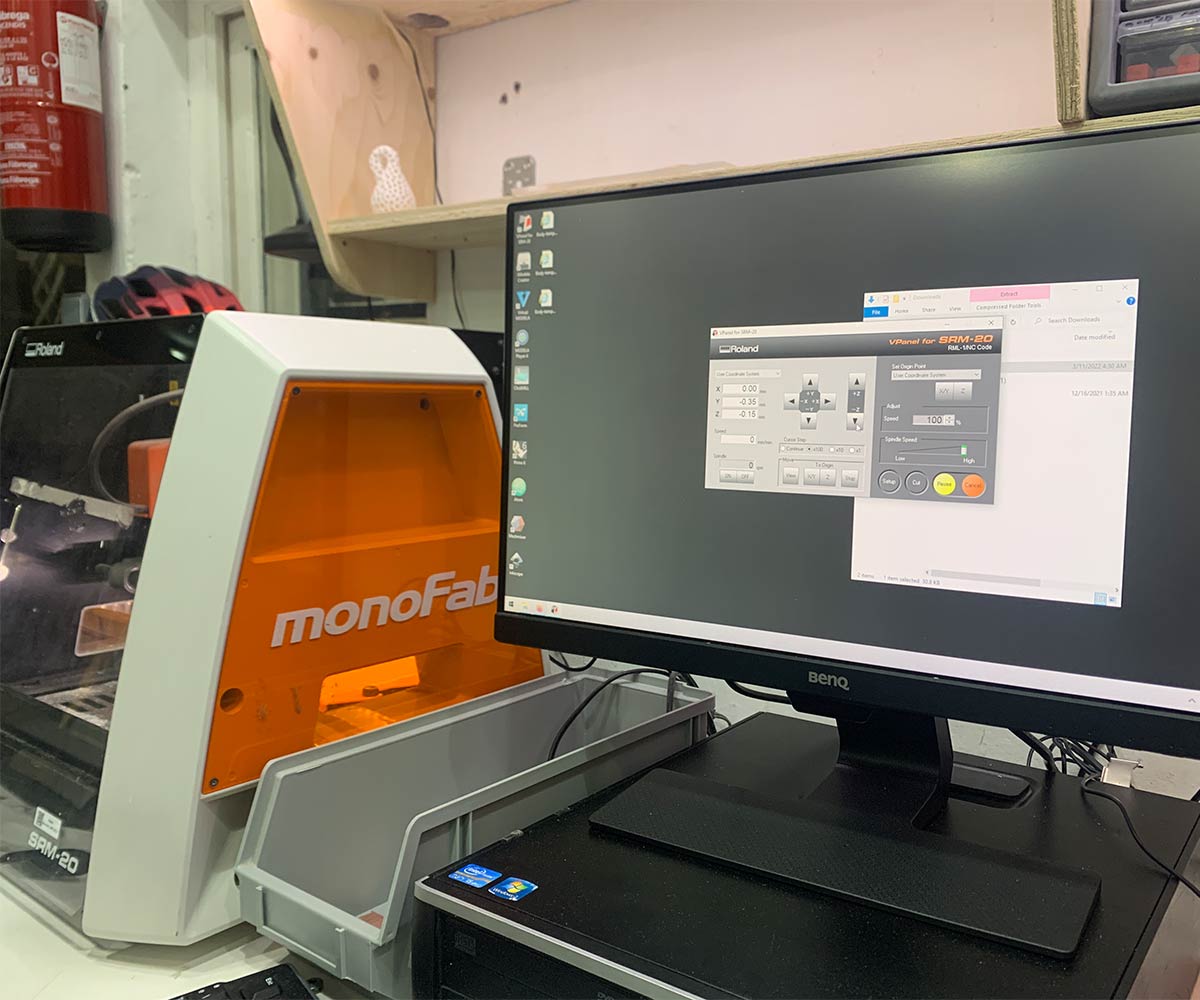
18. Once we got the files ready with the G-code. We go to the PCB milling machine.
19. In this case I used the Monofab SRM
20. Before cutting go to setup and check RML-1/NC CODE and mm are selected.
20. Tape with double facing tape the PCB.
21. Set the axes. X, Y and Z zeros. Unscrew the mill to set the Z, very carefully till it touches the PCB.
22. Once everything is ready send first the traces files with the 1/64 mill, then Change the mill for 1/32 for the holes followed by the outline.
23. Clean the machine and mills and all the files out of the computer.

Interactions process
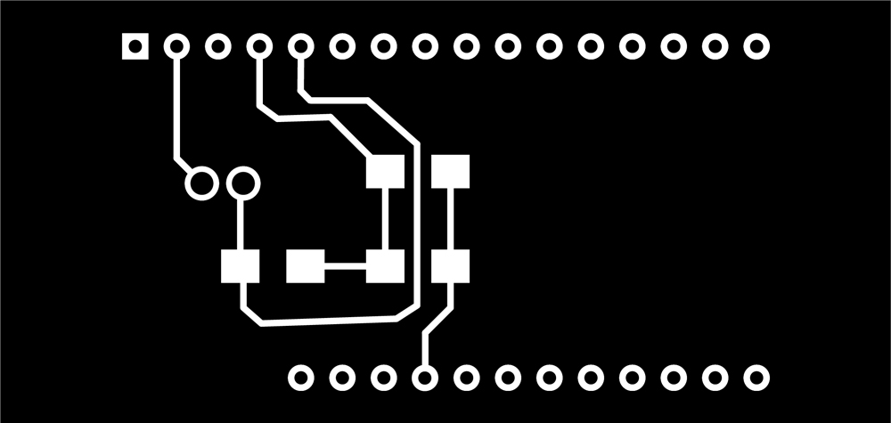
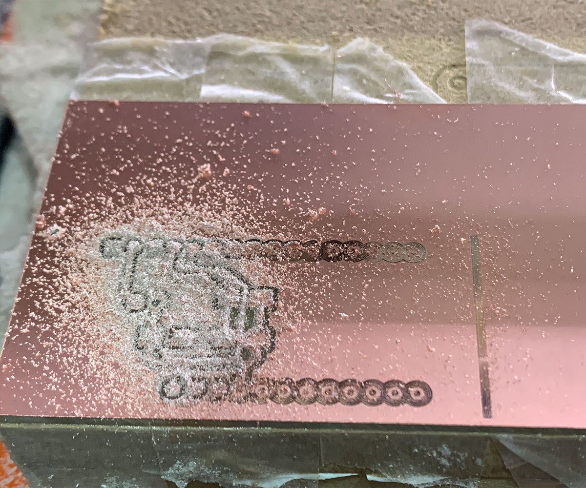
After cutting the PCB, Josep highlighted that I might. have problems with it. As you can see in the picture I separated the circles framing the holes from the traces. Which lead me to mill really big holes without connections to the paths to the components. I understood the issue and designed again the PNG files and sent them to Modsprojects and repeated the process.

This time I found some other issues setting the Z axes. I repeated the process and it was fine, but sometimes after other cutting the sacrificed board can be irregular, so in some areas, the mill wasn’t going all the way through. Josep taught me another technique to set the z with the milling on. Afterwards, I kept having an issue. One of the holes wasn’t being drilled. Edu told me that sometimes mods don’t process the png correctly and one hole wasn’t appearing in the g-code. We can do a small trick and reduce manually the diameter of the mill.
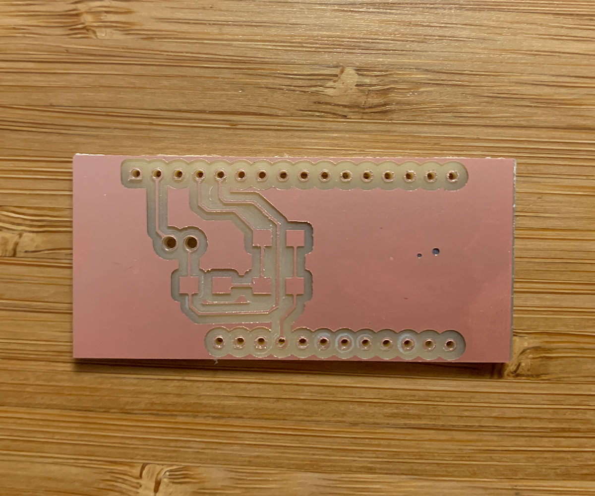
Finally! I got my PCB ready to be soldered the next lab life.
This circuit, might be simple. But I did learned a lot on the process of fabricating it. Eventually I think that in my case would be even more interesting to build future circuits with vinyl copper as I've mentioned before, but for now I just want to experiment.